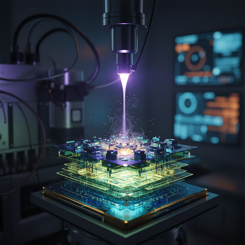
| Physical Vapor Deposition (PVD) | A vacuum process where materials are vaporized and condensed onto a substrate. | Semiconductors, optical coatings | High purity films, good adhesion. | Line of sight limitation, slower deposition rates. |
| Chemical Vapor Deposition (CVD) | A chemical process used to produce thin films by reacting gaseous precursors. | Microelectronics, solar cells | Uniform thickness, excellent conformity. | More complex chemistry, potential toxic byproducts. |
| Atomic Layer Deposition (ALD) | A thin-film deposition technique that alternates between surface reactions to build films one layer at a time. | High-k dielectrics, nanostructures | Extremely precise thickness control, excellent uniformity. | Slower deposition rates, higher equipment costs. |
| Electroplating | A process using electrical current to reduce cations of a material from a solution and plate it onto a conductive substrate. | Microfabrication, decorative finishing | Cost-effective for metal deposition, good thickness control. | Requires conductive substrates, can be limited to certain materials. |
| Sputtering | A process where atoms are ejected from a target material due to bombardment by energetic ions. | Thin films for devices, protective coatings | Versatile materials, good for large area coatings. | Potential for target material contamination, line of sight limitations. |
| Laser Ablation | Using a laser to remove material from a solid surface to create thin films or patterns. | Optoelectronics, nanostructures | High spatial resolution, versatile materials. | Material limitations, can be expensive. |
| Langmuir-Blodgett Deposition | A technique that deposits monolayers of material by transferring them from a liquid to a solid substrate. | Organic electronics, biomaterials | Perfect layer uniformity, good control over layer thickness. | Limited to specific materials, slower throughput. |
| Screen Printing | A method using a mesh to transfer ink onto a substrate to create patterns. | Flexible electronics, decorative applications | Cost-effective for large production, suitable for various substrates. | Limited resolution for fine features, material constraints. |
| Spin Coating | A technique where a liquid material is applied to a spinning substrate, creating a thin film as the liquid spreads and evaporates. | Photolithography, protective coatings | Uniform layer thickness, easy to control thickness by spin speed. | Limited to flat substrates, not suitable for thick films. |
| Sol-gel Process | A chemical solution processing that transforms into a solid gel phase via hydrolysis and polymerization. | Glass coatings, ceramics | Low-temperature process, flexible composition control. | Requires careful drying, potential cracking issues. |

 Close
Close